The 8- 16- 32- and 64-bit memory systems are provided so the 808680486 and the Pentium through Pentium 4 microprocessors can be interfaced to memory. Embedded Programming with Intel.

Pdf 4 Bit Processing Unit Design Usingvhdl Structural Modeling For Multiprocessor Architecture
Lines 6 to 10 identify the design entity One_Bit_Buffer with a signal input Signal_In and an enable control input Enable.
. Tappero Free Range VHDL Free Range Factory 2013. Every VHDL design description consists of at least one entity. 16-BIT ADDITION OF TWO NUMBERS.
This post is important because here we breakdown every single detail of the coding process. Processor design is a subfield of computer engineering and electronics engineering fabrication that deals with creating a processor a key component of computer hardware. The CPU will fetch decode and execute each instruction in order to get the final result.
The development of VHDL began with a joint effort by IBM Inter-metrics and Texas Instruments. The microprocessor chips are available at low prices and results in its low cost. 8288 bus controller converts the input control signals S0 S1 and S2 from 8086 into the io and memory transfer signals needed for direct data.
The microprocessors are versatile. The design process involves choosing an instruction set and a certain execution paradigm eg. 1985 VHDL Version 72.
Since 1987 VHDL has been standardized by the Institute of Electrical. 8 BIT ALUvhdl FREQUENCY DIVIDER USING PLLvhdl 4 BIT SLICED PROCESSOR vhdl IMPLEMENTATION OF ELEVATOR CONTROLLER. The Z flag is set when an ALU operation results in a 0 output.
1 bit addition is the simplest designing process and its internal circuit is also easy to fabricate on the chip. This mode would now require additional circuitry such as 8288 bus controller for translating the control signals. The Department of Defence wanted to make circuit design self-documenting.
8 x 8 multiplier using ADDSHIFT. VLIW or RISC and results in a microarchitecture which might be described in eg. Embedded System Design for Zynq SoC.
It is a small size chip and hence portable. The final version of the language under the government contract was released. You can expand in on this to code virtually any ALU.
Here the whole chip of 16 bit adder is divided into four modules of 4-bit adders. Designs described in HDL are independent of technology very easy for designing and debugging and are normally more useful than schematics particularly for large circuits. 1 bit addition is the simplest designing process and its internal circuit is also easy to fabricate on the chip.
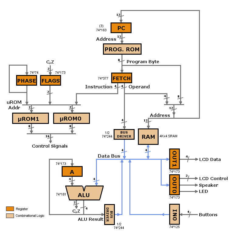
A simple Pseudo-Microprocessor model is used which contains seven instructions ESD book figure 37. Now connecting all the last four adders we can design a 4-bit adder and moving on. Chapter 10 explains memory interface using both integrated decoders and programmable logic devices using VHDL.
Now connecting all the last four adders we can design a 4-bit adder and moving on we can design a 16-bit adder. Lines 12 to 26 identify the design architecture. The firmware a program that executes in a dedicated way and with a specific purpose in a microcontroller or microprocessor is usually stored in a persistent memory device like a NANDNOR flash or EEPROM.
Lines 1 to 4 identify the libraries and packages to use. In this post we will be coding a. JTAG is a physical hardware interface that makes it possible among other things to extract the firmware image from electronic devices.
VHDL Coding for FPGAs. It is a language used for describing a digital system such as a network switch a microprocessor a memory or a flip-flop. Further dividing the 4-bit adder into 1-bit adder or half adder.
We can describe any digital hardware by using HDL at any level. The VHSIC Hardware Description Language VHDL is a hardware description language HDL that can model the behavior and structure of digital systems at multiple levels of abstraction ranging from the system level down to that of logic gates for design entry documentation and verification purposes. View Course Path 8085 Microprocessor MCQ Quiz Interview Questions Published March 7 2020 Updated April 23 2020.
The 8085 has five sign flags. Microprocessors are manufactured by using metaloxide semiconductor technology which has low power consumption. 8086 microprocessor works in maximum mode when its pin 33 MNMX is connected to ground.
Well start off coding an ALU using VHDL in a series of progressions. Further dividing the 4-bit adder into 1-bit adder or half adder. VHDL was developed by the Department of Defence DOD in 1980.
A nibble corresponds to. An ALU or an Arithmetic Logic Unit is the part of a microprocessor that performs the arithmetic and logical operations. For test purposes a.
ME VLSI DESIGN LAB2. VHDL Coding for FPGAs. The RT level design method from previous examples is used again to construct this microprocessor.
The tristate buffer can be created in VHDL using the If-then-else statement as shown in Figure 660. Here the whole chip of 16 bit adder is divided into four modules of 4-bit adders. Mealy Digital McLogic Design Free Range Factory.
Pdf 4 Bit Processing Unit Design Usingvhdl Structural Modeling For Multiprocessor Architecture

Building A 4 Bit Computer From The Ground Up

Building A 4 Bit Computer From The Ground Up

A Complete 8 Bit Microcontroller In Vhdl Fpga4student Com
Design A Simple Microprocessor In Vhdl

Minimalist 4 Bit Processor Focused On Processors Theory Teaching Semantic Scholar
Vhdl Code For 4 Bit Alu
Nibbler 4 Bit Cpu Big Mess O Wires
0 comments
Post a Comment